PCBs, or printed circuit boards, are a crucial component in various types of communication equipment, including smartphones, laptops, and routers. In this blog post, we will delve into the basics of PCBs, their importance in communication equipment, and the key design considerations that engineers must take into account when creating PCBs for these devices.
Importance of PCBs in Communication Equipment
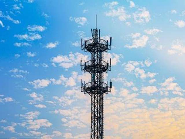
PCBs are an integral part of communication equipment as they provide the necessary infrastructure to transmit and process signals. In smartphones, for example, PCBs are used to connect the various components of the device, such as the processor, memory, and display, and to facilitate communication between these components and the outside world through the antenna and other interfaces.
PCBs are also used in other types of communication equipment, such as laptops, routers, and servers, to connect and control the various components of these devices.
PCB Design Considerations for Communication Equipment
Designing PCBs for communication equipment poses several challenges due to the high-speed nature of the signals being transmitted and the need for impedance control. Engineers must also consider factors such as electromagnetic interference (EMI) and thermal management, as well as size and weight constraints, and the reliability and durability of the PCB.
High-speed signal transmission and impedance control are essential for effective communication in modern devices. The impedance of a PCB trace is determined by its width, thickness, and dielectric constant, and it must be carefully matched to the impedance of the components and connectors to minimize signal reflections and maximize signal integrity.
EMI can disrupt the performance of communication equipment by causing interference in the signals transmitted through the PCB. Engineers must take measures such as using shielded cables and incorporating EMI filters into the PCB design to mitigate EMI.
Thermal management is also crucial for communication equipment as the high-speed signals and dense component placement can generate significant amounts of heat. Proper thermal management through the use of heat sinks and thermal vias can prevent overheating and ensure the reliable operation of the equipment.
Size and weight constraints are important considerations for portable devices such as smartphones and laptops, where the PCB must be as small and lightweight as possible while still meeting the performance requirements.
Finally, the reliability and durability of the PCB are crucial for communication equipment that must operate continuously and withstand the rigors of use. Engineers must select materials and design the PCB to withstand the environmental conditions in which the equipment will be used, such as temperature, humidity, and vibration.
Telecom PCB Assembly Service
Telecom PCB (printed circuit board) assembly is an integral part of the telecom industry, as it enables the production of electronic devices and systems that facilitate communication and data transfer. In this blog post, we will delve into the details of telecom PCB assembly, including its purpose, types, benefits, and the assembly process. We will also discuss quality control measures taken by professional telecom PCB assembly services to ensure the reliability of their products.
What is Telecom PCB Assembly?
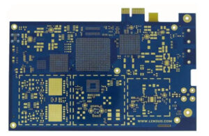
Telecom PCB assembly refers to the process of attaching various electronic components to a PCB to create a functional circuit. PCBs are used in a wide range of telecom devices, including phones, routers, and satellite systems, to name a few.
The electronic components that make up a telecom PCB assembly include things like resistors, capacitors, and integrated circuits (ICs). These components are placed on the PCB and soldered in place to create the desired circuit. The PCB itself is made up of a thin layer of insulating material, with conductive pathways etched onto it to connect the various components.
Types of Telecom PCB Assemblies
There are several types of telecom PCB assemblies available, each with its own unique characteristics and benefits. The three main types are single-layer, double-layer, and multilayer PCBs.
Single-Layer PCBs
Single-layer PCBs are the most basic type of PCB and are made up of a single layer of conductive material. They are typically used in simple electronic circuits where there is a low component density. Single-layer PCBs are cost-effective and easy to manufacture, but they have limited space for components and are not suitable for more complex circuits.
Double-Layer PCBs
Double-layer PCBs, as the name suggests, have two layers of conductive material. They offer more space for components and allow for the creation of more complex circuits. Double-layer PCBs are more expensive and complex to manufacture compared to single-layer PCBs, but they offer improved performance and functionality.
Multilayer PCBs
Multilayer PCBs have three or more layers of conductive material and offer even more space for components. They are the most complex and expensive type of PCB, but they offer the highest performance and are suitable for the most complex telecom circuits.
Benefits of Telecom PCB Assembly Services
Professional telecom PCB assembly services from Eashub offer a range of benefits for companies and individuals in the telecom industry. Some of the key benefits include:
- Cost savings: Outsourcing telecom PCB assembly to a professional service can save companies money on labor and equipment costs. Professional assembly services have the necessary equipment and skilled personnel to manufacture PCBs efficiently and cost-effectively.
- Improved efficiency: Professional telecom PCB assembly services can handle the entire PCB assembly process, from design and prototyping to testing and production. This can save companies time and resources and allow them to focus on other aspects of their business.
- Enhanced performance: Professional telecom PCB assembly services use high-quality components and adhere to strict quality control measures to ensure the reliability and performance of their products. This can lead to improved performance and longer lifespan of telecom devices.
The Telecom PCB Assembly Process
The telecom PCB assembly process involves several steps, including design, prototyping, testing, and production. Let’s take a closer look at each step.
Design
The first step in the telecom PCB assembly process is design. This involves creating a schematic for the circuit and determining the placement of components on the PCB. The schematic is then used to create a layout for the PCB, which shows the exact placement of components and the connections between them.
Prototyping
Once the PCB design is finalized, a prototype is created to test the design and ensure that it is functional. Prototyping allows for any necessary changes to be made before the PCB moves on to the production stage.
Testing
After prototyping, the PCB goes through testing to ensure that it is fully functional and meets the desired specifications. Testing may include electrical testing, functional testing, and environmental testing to ensure the PCB can withstand different conditions.
Production
If the PCB passes all testing, it moves on to the production stage. During production, the PCB is populated with the necessary electronic components and soldered in place. The PCB is then inspected and tested again to ensure that it is fully functional.
Quality Control in Telecom PCB Assembly
Ensuring the quality and reliability of telecom PCBs is essential for the proper functioning of telecom devices and systems. Professional telecom PCB assembly services take a number of measures to ensure the quality of their products.
- Use of high-quality components: Professional assembly services use components from reputable manufacturers to ensure their quality and reliability.
- Strict inspection procedures: PCBs are thoroughly inspected at various stages of the assembly process to catch any defects or issues.
- Testing: PCBs are subjected to various types of testing to ensure their performance and reliability.
- Certification: Professional assembly services may be certified by industry organizations, such as the ISO (International Organization for Standardization), to demonstrate their commitment to quality.
Conclusion
Telecom PCB assembly is a crucial part of the telecom industry, as it enables the production of electronic devices and systems that facilitate communication and data transfer. Professional telecom PCB assembly services offer a range of benefits, including cost savings, improved efficiency, and enhanced performance. They also adhere to strict quality control measures to ensure the reliability of their products. If you are in need of telecom PCB assembly services, consider working with a professional service to ensure the quality and reliability of your telecom devices.